


Purpose
Strain gage testing allows objective analysis of the strain and strain rate levels that a SMT package is subjected to during PWB assembly, test and operation. Characterization of worst-case PWB strain is critical due to the susceptibility of component solder joints to strain induced failures. Excessive strain can result in solder joint damage for all package substrate plating finishes. Such failures include solder ball cracking, trace damage, pad lifting and substrate cracking during board manufacturing and test processes.
 |
 |
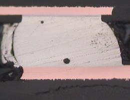
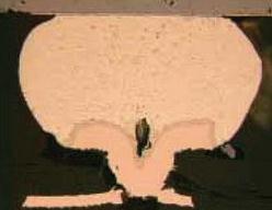
| Solder ball cracking | Trace damage |
 |
 |
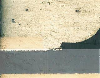
| Pad lifting | Substrate cracking |
Background
Board flexure control using strain gage measurement has proven very beneficial to the electronics industry, and continues to gain acceptance as a method to identify damaging manufacturing processes. However, as interconnect densities have increased and become more fragile, the potential for flexure-induced damage has increased. Many board assemblers are now required to operate under strain levels specified by their customers or component suppliers.
As strain measurement technology has matured, different methodologies have developed. Variations in strain gage methodology inhibit reliable data collection and prevent data comparison across the industry. This document addresses variations in gage mounting, gage placement, experiment design, data acquisition system variables, and strain metrics.
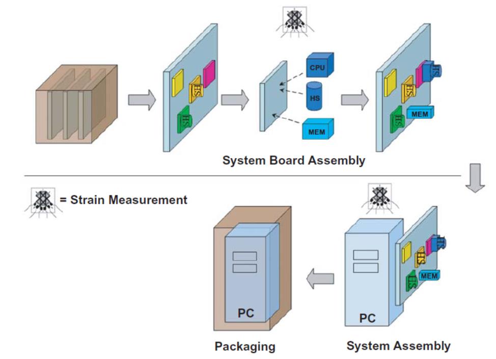
Manufacturing steps that are typically characterized are listed below:
Board Assembly Strain Measurement
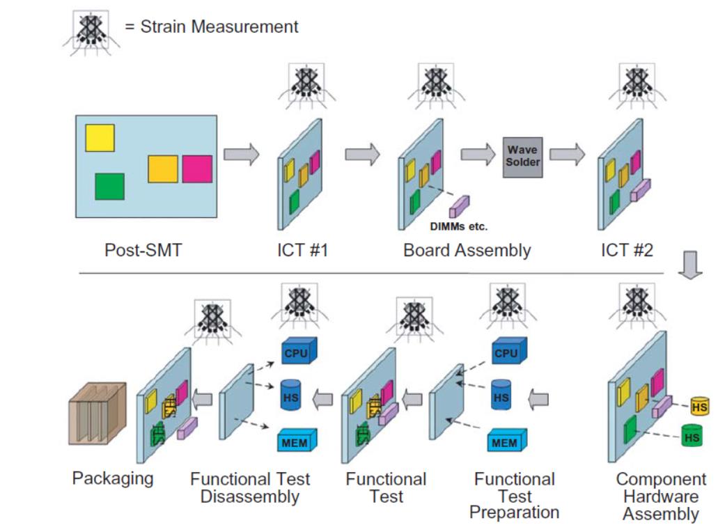
System Assembly Strain Measurement
.jpg) |
The Elogger™ Strain Measurement System is special design for printed wiring board strain testing application. The real-time data provided by the Elogger system avoid the risk such failures include solder ball cracking, trace damage, pad lifting and substrate cracking during board manufacturing and test processes. It meets hardware requirement of IPC/JEDEC 9704. |
.jpg) |
NMB Strain Gage meets hardware requirement of IPC/JEDEC 9704. The product is available in a variety of sizes and design. |
 Language
 Search
 Inquiry Cart